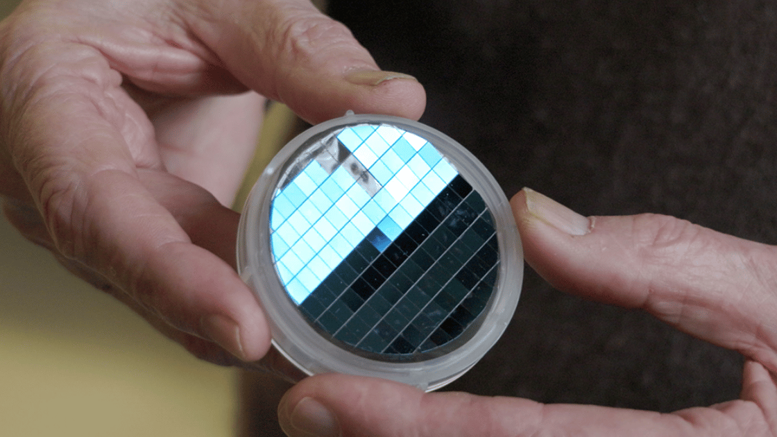
The world’s first functional semiconductor, made from graphene, a single sheet of carbon atoms held together by the strongest bonds known, has been created by the researchers at the Georgia Institute of Technology. Smaller and faster devices could be possible with this technology. This may have applications for quantum computing. Semiconductors, which are materials that conduct electricity under specific conditions, are fundamental components of electronic devices.
The breakthrough of the team throws open the door to a new way of doing electronics. This innovation, led by Walterde Heer a renowned physicist at Georgia Tech, is not merely an incremental step but a substantial leap forward in the field.

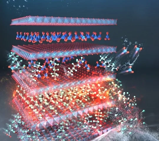
A marvel of material science, graphene is a one-atom-thick sheet of carbon atoms arranged in a hexagonal lattice. Exceptional strength, remarkable flexibility, and unparalleled electrical conductivity—the extraordinary properties of graphene have long made it a subject of intense research. A band gap was a missing element that hindered the journey of graphene towards being a practical semiconductor. This electronic property is essential for a material to function as a semiconductor, allowing the switching on and off of electrical current necessary for digital computation.
We now have an extremely robust graphene semiconductor with 10 times the mobility of silicon, and which also has unique properties not available in silicon. But the story of our work for the past 10 years has been, ‘Can we get this material to be good enough to work?
Walter de Heer, Regents’ Professor of physics at Georgia Tech
The breakthrough of De Heer’s team lies in their ability to endow graphene with this crucial band gap. A sophisticated process of growing epitaxial graphene on silicon carbide wafers enabled this achievement. The method of the team involves heating these wafers to high temperatures, causing the silicon to evaporate and leave behind a graphene layer. The desired semiconducting properties are exhibited by this graphen when produced under precise conditions.

The graphene semiconductor’s electron mobility is one of the most striking outcomes of this research. It is ten times greater than that of silicon. This means, in layman’s terms, that electrons in graphene move with significantly less resistance, leading to faster and more efficient computing.
Similar Posts
As the demands for smaller and quicker electronic devices continue to escalate, this property is especially crucial, pushing the limits of current silicon-based technology. This groundbreaking development also holds promise for quantum computing. The unique properties of graphene facilitate the exploitation of the quantum mechanical wave nature of electrons, a prerequisite for developing quantum computers.
A long-standing problem in graphene electronics is that graphene didn’t have the right band gap and couldn’t switch on and off at the correct ratio,” said Ma. “Over the years, many have tried to address this with a variety of methods. Our technology achieves the band gap, and is a crucial step in realizing graphene-based electronics.
Walter de Heer, Regents’ Professor of physics at Georgia Tech
The challenges remain despite these exciting developments. Scaling up this technology for practical, commercial applications is not trivial. Further refinement is needed for transistor size, quality, and manufacturing techniques.
The existing global infrastructure for silicon chip production, furthermore, poses an economic challenge to the widespread adoption of graphene semiconductors. Graphene represents the potential next step in a long line of advancements in the broader context of electronic material evolution, from vacuum tubes to silicon.
Its development is akin to the Wright brothers’ first flight—a seminal moment, marking the dawn of a new technological era. It is important to recognize the immense potential of hraphene semiconductors and the hurdles that lie ahead as we stand on the cusp of this exciting development.
Involving not just scientific innovation but also economic and infrastructural considerations. The journey from laboratory to widespread commercial use is complex and multifaceted.


