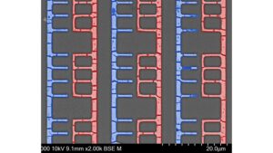
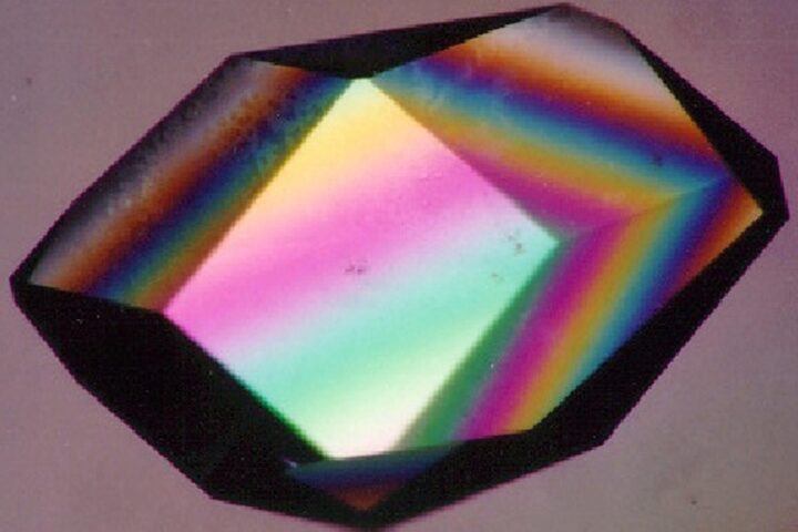
A research team at North Carolina State University has developed a novel technique for manufacturing electronic components. The method, called Directed Metal-Ligand (D-Met) reactions, creates complex three-dimensional structures using liquid metal particles and carbon-oxygen ligands.
“Existing chip manufacturing techniques involve many steps and rely on extremely complex technologies, making the process costly and time consuming,” says Martin Thuo, professor of materials science and engineering at North Carolina State University and corresponding author of the study. “Our self-assembling approach is significantly faster and less expensive.”
The D-Met reaction process begins with liquid metal particles made from Field’s metal – an alloy of indium, bismuth, and tin. These particles are positioned next to a mold of any desired size or pattern. A solution containing carbon- and oxygen-based ligands is then applied, harvesting ions from the liquid metal surface and arranging them in specific geometric patterns.
As the solution flows into the mold, the ion-bearing ligands self-assemble into three-dimensional structures while evaporation packs them closer together. The mold constrains this assembly, creating predictable, symmetrical arrays instead of chaotic patterns. Heating the final structure breaks down the ligands, allowing metal ions to form semiconductor metal oxides while carbon atoms create graphene sheets.
The technique produces consistent results with less waste than current methods. “Current manufacturing techniques have low yield, meaning they produce a relatively large number of faulty chips that can’t be used. Our approach is high yield – meaning you get more consistent production of arrays and less waste,” Thuo explains.
The process requires fewer steps and simpler technology compared to conventional chip fabrication methods.
Similar Posts
The researchers demonstrated the technique by creating nanoscale and microscale transistors and diodes. The graphene sheets produced during the process can tune semiconductor bandgaps, controlling their responsiveness. The inclusion of bismuth allows for photo-responsive structures, enabling light-based manipulation of semiconductor properties.
“The nature of the D-Met technique means you can make these materials on a large scale – you’re only limited by the size of the mold you use,” says Thuo. “You can also control the semiconductor structures by manipulating the type of liquid used in the solution, the dimensions of the mold, and the rate of evaporation for the solution.”
The research team’s next step involves creating more complex devices, particularly three-dimensional chips. Their findings are published in Materials Horizons under the title “Guided Ad infinitum Assembly of Mixed-Metal Oxide Arrays from Liquid Metal.”
The research received support from the National Science Foundation Center for Complex Particle Systems under grant 2243104. Chang, Martin, and Thuo are pursuing patents related to the D-Met research, while Chang, Ward, and Du have a separate pending patent connected to the technology.
This new manufacturing technique adds to the semiconductor industry’s options for producing electronic components through self-assembly methods.
